For years I’ve been saying that, as more and more workloads migrate to the cloud, the mass concentration of similar workloads make hardware acceleration a requirement rather than an interesting option. When twenty servers are working on a given task, it makes absolutely no sense to do specialized hardware acceleration. When one thousand servers are working on the task, it certainly makes sense to do custom boards and/or Field Programmable Gate Arrays (FPGAs). But one thousand is actually a fairly small number in the cloud. When there might several hundred thousand servers all running the same workload, hardware specialization goes from an interesting idea to almost a responsibility. Hardware acceleration can reduce latency by a factor of ten, decrease costs by a factor of ten and, it’s better for the environment, with power/performance improved by at least a factor of ten.
In the 80s I argued that specialized hardware was crazy and the future of our industry was innovative software on low-cost, commodity, general-purpose processors. For many decades that certainly appeared to be true and I’ve managed to make a respectable living on that basic approach: improving performance, availability, and lowering costs by using large numbers of commodity processors. If I ever was correct on this point, it’s certainly not true any longer. We are entering the era of hardware acceleration.
In actuality hardware acceleration has been around in large numbers for a considerable length of time. Commercial routers have massive Application Specific Integrated Circuits (ASIC) at the core. Many specialized network appliances have workload specialize hardware doing the heavy lifting. Most network Interface cards have ASICs at the core. The most effective BitCoin mining engines are using hardware workload acceleration in custom ASICs.
It really wasn’t that long ago that that X86 processors didn’t include floating point on die and it was either done in software on in a separate floating point co-processor. In the somewhat more distant past, I’ve worked on processors that even lacked a fixed point multiply instruction. In the early days of high-performance computing, matrix work was done in software. Cray moved it into hardware with the Cray 1 vector units and, as the cost of a transistor continues to plummet, even hardware vector units are now standard fare in a modern X86 processor.
Hardware acceleration isn’t new, but the operations being accelerated are moving up from the incredibly primitive to replacing ever larger hot kernels of higher-level applications. In the early days, adding the MultiplyAdd (also called Fused-Multiply Add or fmadd) instruction to IBM POWER was a reasonably big deal in allowing the two operations to be done as a single instruction rather than as two. Over time, more hardware accelerations like cryptography have been creeping into general purpose processors and I expect this process will not just continue but pick up pace. General purpose processors have the die real estate to spare and, even if the accelerators are used rarely, with 10x gains across many dimensions, hardware acceleration makes excellent economic sense. In fact, as Moore’s law slows, higher-level hardware acceleration will become one of the most important ways that the next processor generation shows material advantage over the previous.
While general purpose processors will continue to get more higher–level accelerations, another trend emerging much more broadly over the last ten years is the offloading of important workloads from the general-purpose processor entirely. Where a workload has both high value and massive parallelism, it’s a candidate for migration off of general purpose processors and onto graphics processors. It turns out the massive parallelism required for advanced computer graphics also supports some non-graphical workloads incredibly well. Some of the first examples I came across was the offloading of hot financial calculations and the acceleration of seismic studies used in oil exploration. These were important, but the golden workload that has absolutely exploded the general purpose graphics processor market is machine learning. Training neural networks is a highly parallel task that runs incredibly well on graphics processors. Five years ago there was lots of talk about this and some were doing it. Today, it’s hard to justify not running these workloads on General Purpose Graphics Processor Units (GPGPUs) once the workload is being run at scale.
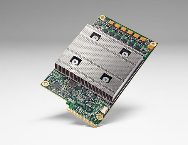
As an example, the Nvidia Tesla K80 GPGPU board has 2 sockets with 2496 CUDA cores each and the overall system is capable of 8.74 TFLOB. The individual cores aren’t that powerful nor amazingly fast but, if the workload is highly parallel, there are a lot of cores available to host it. This part is a bit power intensive at 300W TDP (thermal design power) but that’s not really a problem. What’s both a massive problem and proof of how well this systems supports some workloads is the price. The retail price of the K80 when announced was $5,000. This board is just about as close as our industry gets to pure profit margin with a complete disregard to cost so large discounts are available. But, regardless of discount, this board will never be confused for a low-cost or commodity part.
The good news is our industry is self-correcting and there are many new solutions under development. In fact, partly because the price of this part is so crazy high and partly because cloud volumes are now large enough to justify customer processors, we are going to see more and more workloads hosted on custom ASICs. 15% of the 2016 ISCA papers were on machine learning hardware accelerators and Google, Microsoft, and Amazon all have digital design skills. Not much has been written about the semiconductor work done by the mega-providers but, as an example, at AWS we deploy many hundreds of thousands of custom ASICS each year.
I just read about another excellent example higher-level application acceleration. In fact this best example I’ve seen publicly disclosed so far. The paper “In-Datacenter Performance Analysis of a Tensor Processor Unit” will be presented at the upcoming 44th International Symposium on Computer Architecture (ISCA) to be held in Toronto Canada June 26, 2017.
In my opinion, this is excellent work, a well-written paper, and a balanced analysis of what they produced and started to deploy back in 2015. It’s the normal practice in our industry to only show that which has already been replaced or is about to be replaced but that’s just the reality of commercial innovation and I do the same thing myself.
What I found most striking is the elegant simplicity of what has been done. It wins over general purpose Intel processors and Nvidia GPGPUs of the same generation by the greater than 10x we would expect and yet, they have kept the part simple and shown good taste in what to include and what not to. The paper uses power/performance as a proxy for the price/performance they know they should be using but since this is commercial innovation, pricing needs to remains confidential.
Because the part and board have been in production since 2015, they will have likely done more than 10^6 volume by now. Since the volume is good by semiconductor standards and the part is not that complex, I would speculate that the part is less than $50 and the full PCIe board will cost under $100. For machine learning inference, this part is more than an order of magnitude faster than an Nvidia GPGPU while being more than an order of magnitude less expensive. This is the power of workload hardware specialization and we are going to see a lot more of this over the next decade.
Some key speeds and feeds from the paper:
- 65,536 8-bit Multiply-Accumulate matrix multiply unit
- 92 TeraOps/second
- 28 MiB software-managed on-die memory
- 15x to 30x faster than contemporary GPU (Nvidia K80) or CPU (Haswell)
- 30x to 80x higher TeraOps/second/watt than CPUs or GPGPUs
- System is actually memory bound on four of the six neural net applications so the next part, if you assume improvements at roughly the same speed as CPUs and GPGPUs, would achieve a 70x the performance/watt of the comparable GPGPU and 200x with the comparable CPU
Some interesting observations and lessons learned from the paper in bold with my short form notes in italics:
- Fallacy: NN inference applications in datacenters value throughput as much as response time: Machine learning training values throughput but most inference applications are customer facing where response time is a primary concern.
- Fallacy: The K80 GPU architecture is a good match to NN inference: The K80 and the shorter word length K60 are good but expensive hosts for training. For inference they are only marginally better than general purpose CPUs so their high costs ends up dominating.
- Pitfall: Architects have neglected important NN tasks: 15% of the 2016 ISCA papers were on Neural Net accelerators further underlining my point above. This underlines my point that the solution to the GPGPUs are coming soon.
- Pitall: For NN hardware, Inferences Per Second (IPS) is an inaccurate summary performance metric: Our results show that IPS is a poor overall performance summary for NN hardware, as it’s simply the inverse of the complexity of the typical inference in the application (e.g., the number, size, and type of NN layers).
- Fallacy: The K80 GPU results would be much better if Boost mode were enabled: Setting aside the negative impact of K80 Boost mode on TCO (Section 3), we measured it on LSTM1. Boost mode increased the clock rate by a factor of up to 1.6—from 560 to 875 MHz—which increased performance by 1.4X, but it also raised power by 1.3X. The net gain in performance/Watt is 1.1X, and thus for LSTM1, boost mode would have a minor impact on our energy-speed analysis.
- Fallacy: CPU and GPU results would be comparable to the TPU if we used them more efficiently or compared to newer versions: We originally had 8-bit results for just one DNN on the CPU, due to the significant work to use AVX2 integer support efficiently. The benefit was ~3.5X. It was less confusing (and space) to present all CPU results in floating point, rather than having one exception, with its own roofline. If all DNNs had similar speedup, performance/Watt ratio would drop from 41-83X to 12-24X. The new 16-nm, 1.5GHz, 250W P40 datacenter GPU can perform 47 Tera 8-bit ops/sec, but was unavailable in early 2015, so isn’t contemporary with our three platforms. We also can’t know the fraction of P40 peak delivered within our rigid time bounds. If we compared newer chips, Section 7 shows that we could triple performance of the 28-nm, 0.7GHz, 40W TPU just by using the K80’s GDDR5 memory (at a cost of an additional 10W).
- Pitfall: Performance counters added as an afterthought for NN hardware: 106 performance counters were not enough.
- Fallacy: After two years of software tuning, the only path left to increase TPU performance is hardware upgrades: More yet remains to be done in the compiler to further support the part but I’ll still bet a new TPU is coming soon if not already in production.
This is really fine work by Norman Jouppi, Cliff Young, Nishant Patil, the always excellent David Patterson, and others. If you can find the time, go ISCA2017 in Toronto and, for sure, read the paper: In-Datacenter Performance Analysis of a Tensor Processing Unit.
Really very Interesting and innovative….
Very Interesting article. For the ML workloads with HW accelerators (GPU, FPGA), what is the impact on datacenter networking? Will the traditional leaf-spine DC network architecture needs to change? Not sure if these workload will also affect inter-DC networking.
Rao asked about the impact of big coprocessors and especially GPUs on the data center network. Networks are improving fast right now with it being fairly easy to add cost effective per server bandwidth. Most operators are operating at 40G or 25G and it’s easy to add bandwidth by just adding more channels. For those running at 25G, it’s remarkably affordable and provisioning 50G or even 100G per server isn’t difficult.
There are even fairly substantial gains possible in network latency using SR-IOV. Direct application space networking requires application changes to exploit but it’s the single biggest latency improvement that is easily available. With all these improvements in networking, meeting the capacity requirements of modern workloads isn’t challenging. Latency improvements are bounded by the speed of light, but big improvements are still available with more work. Even with all these networking improvements available, for highly coupled workloads, a single big server will always beat many network connected servers. Multiple servers network connected is the only way to get availability and to scale without bounds but it’s remarkable what can be done in a single server.
Single server configurations with 8 GPU boards each with 2 GPUs is pretty common and larger are possible. The only downside of this approach is all the data moving between GPU boards has to be over the PCIe interface. It’s a bottleneck and forces a copy-in/copy-out coprocessor programming model. It would be far superior to allow the co-processors and processors to share the same server-wide memory space by having all participate in the same cache coherent processor interconnect. On this model, all data in server memory can be operated on directly.
Unfortunately, Intel has been unwilling to license access to the processor interconnect to competitors so this ideal configuration isn’t possible with Intel servers. Nvidia took an interesting approach to this situation by developing their own processor interconnect network, NVlink. Using this approach, all the GPUs in the server are connected by a high speed bus. This further ramps up what’s practical in a single server.
The POWER processor isn’t much of a player in the server with something approaching zero market share. However, it remains a nice server processor and, in the coprocessor equipped server world, POWER has at least one substantial advantage. They can support the same NVLink coherent interconnect and all processors and coprocessors can have cache coherent access to the entire server address space. I love this mode but, even with the more common Intel processor equipped servers, the graphics boards can all be interconnected using NVlink. In that configuration, it’s remarkable how far up workloads can scale before needing to go multi-server. For those workloads that do need to go multi-server, providing the networking bandwidth is not unreasonably expensive or difficult.
Very relevant paper. I am wondering if there is an aplication requiring embedded deep learning, multiplying GPU channel is not afordable, while increasing computatn power. How about the memory capacity and dpeed required?
Sure, absolutely. Deep learning requires two steps: 1) training and 2) inference. Training is still usually done on general purpose CPUs or GPUs. In the case described in the paper under discussion, training is still done on expensive GPUs. The TPU is handling inference. Building an inexpensive inference engine allows it to be deployed very widely — likely to every machine in the fleet.
This isn’t really an embedded application but it has some overlap in characteristics. When going super broad, you need very low cost and the power/performance has to be excellent. Same with embedded applications of ML.
There is no question that there are applications needing inference at the edge in embedded devices and the most price/performing and power/performing solutions will be custom ASICs.
Probably another indication how important FPGA technology has become is that Intel put out $16 billion last year to buy Altera. Clearly this investment has to pay off in the future. FPGA technology is somewhat cyclic (at least in “high-end” compute). There was an initial wave around 2008 with great technology from Cray, SGI, SRC, Nallatech and other companies. Lots of good conferences and momentum to create some form of a standard to exchange IP. Impulse-C, Celoxia, Mitronics all doing really great work. Within a year you could see interest fading away moving to GPU computing. There were a couple of good reasons (large-scale FPGAs were expensive, somewhat hard [to put it mildy] hard to program and required truly massive parallelism to be comparable to CPUs running at > 2.5 GHz. Building real heterogeneous programs (executing in parallel on multiple cores plus FPGA instead of a pure offload model) is still hard. I remember we did a lot of “Tupperware” workshops mostly with academics where we showed with partners how to write “hello world” on a FPGA platform. Once you overcome this hurdle it’s getting a lot easier. If you leave a Fortran or JAVA programmer alone, try to figure out why his algorithms should consider signal propagation delays in the implementation, well it’s tough. While ML is taken a prime spot today, there are other well suited applications like DNA matching etc where it’s really great that you can choose 5 bit arithmetic as example which then allows to implement more ALUs on the chip.
Creating a market place of IP implementations is a very smart move connecting design houses with specific user needs, at least in my view
Mathias said “Intel put out $16 billion last year to buy Altera. Clearly this investment has to pay off in the future.”
I would argue that a great many mega-companies have made massive investments that never paid off so this one isn’t assured. But, like you, my money is with Intel. I think investing in FPGAs is super smart. Much of the future generational gains Intel will bring to market will be hardware accelerations. The trick will be to find these accelerations, chose to implement those with the broadest use. Even if no customer uses the FPGAs comming in Intel processors, they would be a great tool for Intel. They can use the FPGAs to test new accelerations in partnership with customers. They can measure gains on real workloads and decide to implement the successful accelerations in hard logic.
Clearly this FPGA will also be used by customers wanting to offload hot kernels from important applications to Si so it won’t be just Intel experiementing with them. But, if I was at Intel, I would be sending out professional service team to key customers to help bring their workloads to FPGAs. Intel will learn far more about real applications workloads, it will be challenging for those customers to move to different processors, and Intel will be choosing the best and most broadly used accelerations for delivery in the next processor generation. Big potential win.
Matthias also made the key point that programming FPGAs is hard and he pointed out that “while ML is taken a prime spot today, there are other well suited applications like DNA matching etc where it’s really great that you can choose 5 bit arithmetic as example which then allows to implement more ALUs on the chip.”
I agree and this is one of the key reasons why AWS is offering the F1 instance type:https://aws.amazon.com/ec2/instance-types/f1/. This AWS instance type hosts up to 8 Xilinx UltraScale Plus FPGAs each with 64 GB of DDR4 ECC DRAM and a dedicated PCIEx x16 connection. This Xilinx part includes 2.5 million logic elements and 6,800 DSPs with good quality development tools.
Totally agree James. Actually the majority of mega-mergers in the tech-industry failed. Tandem, Compaq, DEC … I hope Intel/Altera will work out. You guys are doing an amazing job in the F1 instance, it clearly takes a holistic view of the field, in-depth technology and simply the guts to jump into the water :).
NVIDIA did an outstanding job to bring GPU computing to the masses, focus on training and evangelizing (I hate this term, but it describes well what it takes). The fan-out providing training to universities vs professional service teams working individual customers is better, but you clearly need both. BTW, in my old slide decks talking about FPGAs I had the internal bandwidth of all the blocks RAMs. This is always a mind-blowing number
Exactly Matthias. I too hope the Intel Altera acquisition works out. I can think of many reasons why it should and it’ll open faster hardware innovation. I love F1 because it makes the same tools available to all cloud computing customers. Even more exciting, it’ll make it much less expensive to have university students working with very capable hardware. Anything that reduces the friction in teaching, is good for the industry, the students, and society as a whole.
Hi James. Thanks for your insights here. Its seems that an important characteristic is the power consumption of these platforms. How does this impact which platforms (CPUs, ASICs, GPUs, FPGAs) AWS uses?
Generally FPGAs consume far more power than hard logic but it’s actually kind of hard to state a simple rule that applies everywhere. An FPGA implementing a given algorithm will typically consume less power than a CPU or GPU running a software implementation of that same algorithm. Software on general purpose processors is generally less power efficient than FPGA implementations but, for logic implemented in hard logic whether in a ASIC, GPU, or CPU, the FPGA is far less efficient. What makes it hard to state a hard and fast rule is it depends upon the hardware/software mix. If it’s all in hardware, an FPGA is less efficient than hard logic (ASICs, GPUs, and CPUs) but the system is usually a mix of hardware and software so it really depends on workload, the hardware/software mix, the hardware design, and the process used to implement the logic.
When I see FPGAs in networking gear, there is almost always a very large power cord running out the back :-). However, the two factors are just highly correlated rather than a hard and fast rule. Current graphics processors are performance focused rather than power optimized but that is a design choice and others could easily yield a highly efficient part.
Bob Brodersen (Berkeley) showed that over a very wide range of implementations, GPU’s/DSP’s tend to be ~10x more efficient than general purpose CPU’s, and hard ASIC pipelines another ~100x more efficient than GPU’s. Anecdotally I’ve found that FPGA’s fit nicely in the gap – about 10x better than GPU’s, about 10x less efficient than hard logic. The result tends to be that people try to map the compute intensive parts of the algorithm to something less general, and run the 95% of the code that uses 5% of the compute cycles on the GP machine. That works unless the problem definition changes – at which time there is a very high price for moving functionality to the GP machine.
Good set of general rules of thumb from Bob Brodersen. The only factor that is hard to characterize in a rule of thumb is it depends upon the workload and how well that workload runs on the hardware in question. The two factors I’m after are memory bandwidth and the portion of the workload that is directly supported in hardware in question. If the part is memory bound on a give part, the standard rules are less likely to apply. It makes a big difference if the hardware directly supports the algorithm vs the algorithm mostly being in instructions processed by the hardware. Even ASICs can implement processors that can process general purpose instructions so ASICs can be identical to CPUs and cases could be artificially constructed where FPGAs beat both. Nonetheless, the rules of thumb offered by Bob are good ones to get started in thinking through options.
Hi James. Do you have any opinion on IBM’s TrueNorth processor? 70 milliwatts takes the headlines, but I have no idea of its actual usefulness in the real world.
True North is a research systems exploring what IBM calls “brain inspired computing.” It’s fairly ambitious for a research chip with 4096 cores in 5.4B transistors. They are exploring synaptic computation which are non-von Neumann architectures modeled after the human brain. I’ve never found anything about the programming model and how complex the system is to program and I’ve not come across any problem that the new architecture opens up. It’s still pretty early days in this research effort.
I grew up with the Cray-1 (and later X-MP, Cray-2 etc). They have been pretty versatile systems addressing lots of different scientific workloads. I remember regular discussions why scalar codes would run slow however.
There are a couple of interesting points with the TPU. Clear focus is on inference (and very low latency). I believe this is one key technical point. The other is the statement that massive deployment has saved the construction of 15 data centers. A good sized data center is probably around $150M (?) that’s an economy of $2B. Not bad.
I think the economics behind hardware acceleration for high volume and very latency sensitive workloads in inarguable and we are going to see a lot more workload specific acceleration coming to market.
James, the $50 cost of TPU is PCOS only, right?
Tested die in package in volume without margins.
Hi James, I’m a bit of a laymen, but if you think ML will eventually be half of the world’s server footprint, how do you think that will breakdown before training and inference?
*between not before training and inference
It’s still very early in the machine learning deployment. Massive world-wide workloads have to service a very wide number of concurrent requests and that would seem to wildly favor inference as the dominant of the two. But, on the other hand, for high value workloads, there is no obvious bound on training resources other than hardware cost and the availability of cost of training data. I could imagine workloads that are similar in training expense to search but without needing a massive world-wide foot print of inference engines. These workloads would likely be highly training dominated. It really depends upon the workload, the value of the workload, the complexity of the problem, the availability of cost effective training data, and the complexity of the model. My speculation is, as ML gets more broadly deployed and lower value workloads are taken on, the ratio of training to inference would increase. Certainly it’s easy to imagine workloads where the training costs are comparable those required by internet search but rather than having an inference fleet to support the entire world, there might be only 1 inference being run. I suppose it could be a super expensive model to evaluate :-)
Thanks for the thoughtful response as always James. It will be interesting to watch how this space develops overtime. if you are correct that in 10 years time frame, 50% of all server footprint will be dominated by ML workloads, and since hyperscale companies like Amazon already count as 50% of server purchases each year, and represent the fastest growing server architecture, then by default, ML will be the majority of what’s being run on AWS and other big cloud properties sooner than the 10 years you quoted for the overall server footprint. This begs the question as to whether there is enough uniformity on these ML workloads to have an ASIC for all of them (stripping out workload acceleration that can use FPGAs)? will this ASIC be a companion to CPUs or GPUs/FPGA or flat out eliminate the need for these parts and what their role will be in training vs inference.
Eric asked “is enough uniformity on these ML workloads to have an ASIC for all of them (stripping out workload acceleration that can use FPGAs)? will this ASIC be a companion to CPUs or GPUs/FPGA or flat out eliminate the need for these parts and what their role will be in training vs inference”
The paper targets ML inference only and make a good case that a single hardware platform can cover a very wide range of inference workloads. The paper also argues that inference tends to be response time focused whereas training tends to be throughput focused. This inference engine is sufficiently inexpensive that it could actually be deployed to the entire fleet — adding $100 to perhaps as much as $150 to the entire fleet is expensive but there is very high value in making the entire fleet inference capable.
I’m pretty confident that ML training, just like inference was, will be amenable to specialized hardware and specialized hardware will cover a broad enough swath of the workloads to justify doing custom hardware. The larger and most important of the training workloads today are moving or have moved to to high cost GPUs. This shows there is value in in moving these workloads off general purpose processors onto more specialized, highly parallel systems. I’m speculating that the high profit margins of current generation graphics processors will quickly attract hardware competition focused on machine learning.
I suspect we’ll see specialized hardware behind both ML training and inference but it’s highly likely that it won’t be the same hardware supporting both.
Very interesting article. Thank you. Follow up to your comment, “in 10 years, ML will be more than 1/2 the worlds server side footprint.” In 10 years, in the ML footprint, what type of split do you see between training and inference? And in each segment, what do you think will be the split between GPU, FPGA, CPU, and ASIC enabling the ML?
Sorry, I missed your question Rob B but, fortunately, David asked a similar question above. You also asked about the split between GPU, FPGA, CPU, and ASIC. FPGAs are best for low volume workloads or those that change more frequently than the normal one to two year ASIC cycle. For the volume involved, FPGAs don’t seem a likely bet at least not for the bulk of the market. FPGAs are a good way to experiment with ideas not yet sufficiently well proven or with big enough to justify an ASIC. Although I don’t see FPGAs willing the bulk of the machine learning market, I’m still super excited about FPGAs and very optimistic that they are going to see increased growth. In fact, I’m particularly excited about our decision at AWS to introduce an FPGA instance type in EC2 to allow customers to experiment with putting workload specific optimizations in hardware.
There is really no difference between CPU, GPU, and an ASIC in their ability to support machine learning. Current CPUs don’t have the massive parallelism, small word size, and memory bandwidth that best support these workloads. But, as smaller feature size open up more CPU real estate, it’s highly likely support will be added to general purpose processors. GPUs run training workloads very well today but high price is making room in the market for other approaches and competitors. Inference workloads only run marginally better on a GPU than on a CPU but GPU manufacturers easily could target the inference market and probably would get uptake with a lower priced part. Of course custom ASICs can run these workloads well.
The approach that gets the market share really depends on decisions made early on. Any could win and the market is certainly big enough to support multiple approaches. Historically, the complexity of developing an application ecosystem with good development tools and a rich 3rd party application stack, usually limits the number of semiconductor winners to a small number. And great products like Digital Alpha prove that technically better won’t win without that broad ecosystem support.
Hi James once again this is a terrific article. I especially appreciate the last fallacy and i agree that Google wouldn’t be publishing this paper if not a second gen silicon wasnt’t already planned for production that is likely to show orders of magnitude higher performance than existing first gen.
I am curious on your views on how amzn will move forward on this. I see the logic (pun intended) in using an ASIC strategy in AWS’s networking, including security and storage use cases. It is however less clear to me on how AWS using anything other than CPUs/FPGAs/GPUs for machine learning workloads going forward since they remain small and also there is lack of uniform,large scale use case (for now at least) at AWS as it relates to these nascent machine learning workload that are customer facing. Would expect to move to an ASIC for your deep learning as quickly as GOOGL did? how big you think machine and deep learning workload would become as demand on AWS (GOOGL seems to angle for a big chunk of their demand overtime)? any thoughts on existing/future FPGAs and memory architectures as it relates to AWS environment (what Intel discussed using multi-chip combos of fpga/memory/cpu), is that attractive to AWS?
Thank you
I respect all perspectives but you are way off the mark on some of your assumptions on this one Eric. Specifically, you said ” It is however less clear to me on how AWS using anything other than CPUs/FPGAs/GPUs for machine learning workloads going forward since they remain small and also there is lack of uniform,large scale use case (for now at least) at AWS as it relates to these nascent machine learning workload that are customer facing.” Not the case. Let me take a run at some of what’s currently under way in the company.
A big part of the success of the Amazon.com retail platform has been an machine learning investment that goes back more than a decade. The most successful machine learning platform on the planet, Alexa, is an Amazon product. Alexa is also the most broadly supported platform by third party platform developers. There are many thousands of engineers working on machine learning inside Amazon but, as big as this is, we always expect the external use of AWS to exceed even the massive internal use I described here. AWS had the volume to justify an ASIC investment years ago. We aren’t held back by business case or usage volumes here. In fact, that’s one of the joys of working at AWS. Even in the very early days, I never felt we were held back by volume or businesses case. The leadership is pretty good at jumping on and supporting ideas that help customers and each year I’m blown away by how much the team finds a way to deliver. Never satisfied but truly impressed.
Hi James I appreciate the response. I am certain that the use of machine learning for amazon.com infrastructure as a whole has a very long and well accomplished history as you state and is the reason for Amazon’s success against old economy companies.
My question also was not really about lack of scale preventing Amazon from making the necessary ASIC investment. It was more about a question around if, within AWS, for large customer requirements, that you have identified any workloads emerging specifically tied to machine and deep learning that have reached the stage of maturity and scale that would warrant an ASIC design. This may be something still ahead of Amazon if it believes a future workload merits an ASIC investment. if the answer is all large scale workloads merit an ASIC investment then there has to be an area where Amazon’s investment would have the biggest economic impact. For ex, Google’s investment in TPU is very sound given lack of economically viable commercial products that mirror what TPU does and their view that Google plans to be big for machine learning as a service. Do you have something similar at Amazon that would justify this big investment.
I’m totally following your line of questioning Eric and it makes sense. But there are a couple behind assumptions what you have written that aren’t 100% correct. The first was that hardware is workload specific rather than workload type and so you need a single workload to justify the investment to do hardware. Essentially there many shades of gray between fully general and 100% workload specific.The second assumption is that there were no viable competitors that could support the Google workload so they were forced to do a hardware unit. Let’s look at each assumption in order:
From the original paper, the authors said:
Three kinds of NNs are popular today:
1. Multi-Layer Perceptrons (MLP): Each new layer is nonlinear functions of weighted sum of all outputs ( fully connected) from a prior one, which reuses the weights.
2. Convolutional Neural Networks (CNN): Each ensuing layer is a set of of nonlinear functions of weighted sums of spatially nearby subsets of outputs from the prior layer, which also reuses the weights.
3. Recurrent Neural Networks (RNN): Each subsequent layer is a collection of nonlinear functions of weighted sums of outputs and the previous state. The most popular RNN is Long Short-Term Memory (LSTM). The art of the LSTM is in deciding what to forget and what to pass on as state to the next layer. The weights are reused across time steps.
In the Google example, they report that 61% of their Neural Network Inference workloads are Multi-Layer Perceptron, 5% are convolutional neural networks and 29% are Recurrent Neural Networks (mostly Long Short-Term Memory). The TPU supports all three of these workloads and the paper shows multiple benchmark results from each broad area. Even though “hardware” sounds like fixed workload, that’s not the case. A very broad swath of machine learning inferences problems can be covered quite well by specialized hardware like the TPU.
Your second assumption is that there were no viable competitors to handle these vial workloads so Google had no choice. These workloads are actually well supported by both Intel general purpose processors and Nvidia GPGPUs. In fact up until as recently as 2015 Google ran all these workloads on general purpose processors. They described this workload hosting evolution in the paper:
Starting as early as 2006, we discussed deploying GPUs, FPGAs, or custom ASICs in our datacenters. We concluded that the few applications that could run on special hardware could be done virtually for free using the excess capacity of our large datacenters, and it’s hard to improve on free. The conversation changed in 2013 when we projected that DNNs could become so popular that they might double computation demands on our datacenters, which would be very expensive to satisfy with conventional CPUs.
There are many competitive solutions able to run these workloads with the most common being general purpose processors with GPGPUs somewhat behind. GPGAs and ASICs have advantages and because it is possible to support a large number of diverse machine learning workloads on a single specialized hardware platform, the volumes make sense and economics look very good.
I would expect that all the mega-operators have sufficient workloads to support specialized ML hardware investments today certainly Amazon does.
Thanks James for being gracious with your time and responses.
I was also asking because AWS made the F1 service available, which i understand from a customer demand standpoint but seems to run counter to the view outlined above that ” it is possible to support a large number of diverse machine learning workloads on a single specialized hardware platform, the volumes make sense and economics look very good”. are the economics of providing workload acceleration on FPGA that much more compelling and applicable to lot of AWS workloads than using specialized ASICs?
https://aws.amazon.com/ec2/instance-types/f1/
That’s an excellent question Eric “are the economics of providing workload acceleration on FPGA that much more compelling and applicable to lot of AWS workloads than using specialized ASICs?”
The F1 instance type is one I’ve super proud of and, although most in the industry won’t talk much about it and some customers may not even know what an FPGA is, the F1 instance type is super important from my perspective and it’s one of the ways that AWS is different.
Like many in the industry, we know that hardware acceleration is important for large, very high volume workloads. Hardware took over repetitive, latency sensitive networking workloads many years ago. AWS has deep investments in custom silicon and we are installing many 100s of thousands of these custom ASICs each year. Machine learning workloads are a big part of what we run at AWS today and it’s my belief that these workloads are going to just keep growing and I expect that in 10 years, ML will be more than 1/2 of the worlds server side foot print. All other workloads will continue to grow as they are today but ML will eclipse them all. There is already sufficient volume in ML to justify a hardware investment and my forecast of market size says these workloads are just getting started. Certainly, there will be many hardware investments in support of ML.
Inside AWS, we understand the improvements in price/performance, power/performance, and latency that comes from custom hardware and we are deploying custom ASICs in very large numbers. What makes the F1 instance type interesting is it’s a platform where our customers can do the same thing for their largest and most latency sensitive workloads. If the F1 is as successful as I hope it is, it still won’t do the volumes of a C-type instance but it will allow AWS customers to do their own hardware acceleration and use it cost effectively in the cloud, the instance type will allow hardware researchers to do inexpensive experiments in hardware and I hope it leads to many more well trained digital designers with real workload acceleration experience, and it’ll also be a platform where smart people in AWS and Amazon.com can experiment with hardware acceleration beside their workloads running on general purpose CPUs and GPUs. I suspect that some of the innovation done on F1 instance types will be related to machine learning since it is massively important but I also suspect the F1 innovation will be far broader and I hope customer and partners target other workload accelerations we haven’t thought of yet.
F1 is us saying, “if hardware acceleration is so incredibly important to the AWS platform price/performance and latency, why wouldn’t it be equally important to our customers and their specialized workloads.” F1 is about us unlocking customers innovation in hardware.