A couple of days back, Ganesh Venkataramanan, leader of the Tesla Dojo project, announced the Dojo machine learning training system. It’s an unusually network rich, power dense, and memory light design. I’ve summarized the architecture of the system below but I found three aspects of the system particularly interesting:
- Massive Network: Each D1 chip delivers 16,000 GBps (4 channels of 4Tbps) of networking and they are combined into 25 chip MCM (Multi-Chip Modules) to deliver 36,000 GBps (4x 9TBps) of network bandwidth
- Tiny Memory to compute ratio: Each D1 chip is made up of 354 functional units and each functional unit has only 1.25 MB of SRAM and no DRAM at all so there is less than ½ GB of memory per D1 processor. They have provisioned large DRAM pools on each end of a 5 rack row there is no DRAM in the compute racks themselves. In thinking through how they can operate so light on memory, I suspect it’s a combination of vast networking bandwidth and that the system is designed to run vision models where are less memory intensive than many other common ML training workloads.
- Massive power density: Each D1 chip only dissipates 400 W which about as expected for a modern part of that size but they have combined these into fairly dense 25 chip MCMs called training tiles each of which dissipates 15kw (10kw of D1s and 5kw of voltage regulators and other overhead). That’s 1.8 megawatts for the full planned 10 rack Dojo training system. As a point of scale a mid-sized datacenter will run in the 30 to 40 megawatt range).
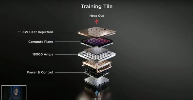
Looking closely at the pictured roughly 1 sq ft training tile above, the top is an aluminum plate presumably to mate up against a phase change liquid cooling system.
It’s a minor point but it’s a nice touch to put the VRDs( Voltage Regulator Down) directly on tile allowing them to deliver an unusually high 52V to power the tile. Given the 15kW draw, that’s still a 288A draw at 52V.
354 Functional units are combined in a single 645 mm^2 D1 chip. 25 D1 chips form a multichip module called a training tile and 12 training tiles form a rack and 10 racks for an Exapod.
Functional Unit:
- 4 thread SMT (Symmetric Multi Thread)
- 512 GBps (4x 128 GBps) network bandwidth
- 1.25MB SRAM
- SIMD matrix unit
D1 Chip: 645mm^2
- 354 Functional Units (training nodes) per D1
- 16,000 GBps (4x 4TB) network bandwidth
- 442.5 MB SRAM
- 2Ghz
- 400W (fairly low)
Training Tile: ~1 sq ft
- 25 D1 Chips
- 36,000 GBps (4x 9TB) network bandwidth
- 11GB SRAM/tile
- VRD on wafer with 52VDC input
- Full mechanicals to manage 15kW
- 10kW from 25 D1s and 5kW from VRDs and other overhead)
Cabinet (rack):
- 12 Training Tiles per rack (2 trays of 6 per tray)
- 132GB SRAM/rack
- 180kW/rack
Exapod: 10 racks
- Still full 36TBps between each module
- Each 5 rack pod has general purpose CPUs on either side with large DRAMs pools
- 4 DRAM pools on full 2 row, 10 rack Exapod
- 1.32TB SRAM/Exapod
- 1.8MW per Exapod
It’s quite an innovative system. More details at: Tesla’s AI Chip Revealed
I am guessing that the large DRAM pools at the end (@exapod level) are not HBM-DRAMs. With super-high-BW-proprietary network near their D1 chips, the bandwidth is already taken care of. I am guessing that the DRAM pools are DDR3/4 based DIMMs acting as level-N cache.
James, can you please confirm?
I’m pretty sure your guess is correct — there would be no point to pay more for HBM once it’s already that far away.
Dojo looks quite similar to Cerebras’ CS-2 from a high level. Thought the Cerebras’ system-level approach (memory pool and interconnect fabric) is very clean and scalable.
Yes, I agree. The systems are remarkably similar. Both systems using massive multi-chip modules, unusually high power density, very high network bandwidth, but only remote memory. I would think that the latency to remote memory will make both systems less than ideal for language models but we’ll see. It’ll be useful to see where the Cerebrus CS-2 gets used most effectively.
I love Elon’s unfettered honesty. After the reveal of this remarkable computer (which I’m guessing they must be many tens of millions into already) he commented “this will be great if it’s faster than our GPU cluster; a complete waste of money if it’s not”. What’s your new job? I was wondering how the AWS changes might impact you…
You’re right Peter. Elon, like many fine IPA beers is unfiltered :-). My favorite example of that genre is a brewery in Halifax Canada where their original brand was “Unfucking Filtered” — they have since cleaned up the brand name to “Unfiltered” but they still have iconic the domain name https://unfuckingfiltered.com/. That’s Elon Musk all the way.
I love many aspects of what the Tesla team has done with D1 and Dojo. It’s true that a data flow machine with so little memory isn’t ideal for many workloads — it’s not a great language model training engine — but, even while being quite specialized, it’s full of courageous engineering decisions that I respect.
I was in the team that did the MasPar MP-1 SIMD mini-supercomputer (the Thinking Machines era) that seemed quite exotic at the time. We designed a custom SIMD processor chip (450,000 transistors!, 70 ns clock cycle) and used state-of-the art 15 layer PCB’s. On the other hand, each processor board only disappeared 50 W. Hard to fathom how much has changed. I hope TESLA succeeds but my experience-influenced intuition wonders if there is too much risk.
They do have a load of risk on this one but they only have to run very large vision training models and they can dedicate the entire machine to a single job. The combination of not having to run larger classes of workloads (especially those that need more memory) and not needing to partition the machine to run concurrent sub jobs increases the chances of them being successful with this machine. My take is they know their workload well and will have run extensive simulations so they are probably well covered as long as workloads characteristics don’t change greatly.
And if they make the hardware work (not to mention reliably enough for multi-day jobs). If you read the Google paper on their first Tensor Flow inference accelerator is was very much designed to accelerate the specific computational kernels in use. DEC research did a famous paper looking at MicroVax real code execution to see the degree that the design — done with standard workloads — worked on real code, and discovered that the chip was completely limited by pin bandwidth so all the internal nuanced optimization was for nothing. Nothing like having the exact code to model.
Yes, memory bandwidth is a common real-world workload limiter. Tesla solved that problem by having no DRAM at all and just pipelining the entire workload through the machine on a super high bandwidth proprietary network.