High Performance Transactions System (HPTS) is a invitational conference held once every two years at the Asilomar Conference Center near Monterey California. My first HPTS was back in 1995 thanks to Pat Selinger. I loved it and attended each one up until 2012 when I started a 10 year around-the-world cruise in a small boat.
It was great to be back at HPTS after a 10 year hiatus. Partly it’s a chance to catch up with old friends and valued colleagues and partly it’s a chance to see interesting work from both industry and academia. HPTS is a special group and most of the value of the conference is the people that attend. Attendees cover the spectrum from students, early career engineers, to Turing award winners. I was asked to do the keynote this year and I elected to cover HPTS Comes Full Circle. I’ve linked to the slides below and the talk summary follows.
HPTS Comes Full Circle
Over the years I’ve been attending HPTS, the meaning of “scale” has changed fundamentally. In the early days, “high-scale” were the transaction processing systems used by the largest enterprises, and at HPTS we talked about how these systems were built and how to keep them scaling. Later, data warehouses and large-scale analytics became the HPTS definition of “large”, and their 2x growth per year became our definition of rapid scaling. In 2001 Charlie Bell and Rick Dalzell spoke at HPTS about Obidos, the core of the Amazon.com ecommerce system. Again, our definition of scale had advanced – these mega-ecommerce systems made the large-scale enterprise systems look tiny.
Eight years later our definition of large had further advanced, and very large search and advertising systems had become our latest definition of “big.” Urs Holzle and Luiz Borroso’s “The Datacenter as a computer: An Introduction to the Design of Warehouse Scale Machines” focused on treating the entire datacenter as a computer. At this scale, custom hardware was possible and most of the hyperscalers were using custom server designs, with a few doing all-custom networking hardware. This revised definition of “high-scale” was a fundamental breakthrough in that we were no longer restricted to software innovation and the new canvas for high scale systems included the entire hardware and software stack.
High-scale cloud computing operates at a scale an order of magnitude beyond internet search and advertising systems and opens up yet another dimension for innovation. Building-scale warehouse computing has given way to regional computing complexes of 10s of datacenter each hosting 80 to 100 thousand servers. The world-wide footprint of the largest operators is many 10s of millions of cores and growing rapidly. The best operators develop their own software, their own servers, and their own networking equipment. None are stuck accepting the slow-paced world of standards, and the scale of a single operator has continued to increase to the point where even custom semiconductors are now possible. In the networking world, companies have emerged whose entire business model is producing custom networking ASICs (Application Specific Integrated Circuits) for hyperscaler cloud computing operators.
The growth rate of the hyperscaler operators has continued to accelerate and the next layer of innovation has opened up: custom general-purpose compute processors. Processor design is incredibly expensive where a single part will require a several hundred-million-dollar R&D program and competitive processors require generations of investments. HPTS innovation now includes the entire software stack, the servers, the networking system, and also the processors that form the servers.
In some ways, we have come full circle where, in the early days of HPTS, we were looking at the crazy low-volume IBM mainframes, assembled into complex systems whose sole purpose was to allow the few very largest enterprises to scale their online transaction systems. These wonderful systems that supported the world’s largest companies in the early days of HPTS were made irrelevant by high-volume silicon, high-volume commodity servers, and open source systems software. The super-optimized server hardware systems were replaced by high-scale clusters of commodity systems available to all customers.
The scale of cloud computing where 10s of millions of cores are purchased each year by a single provider returns us to the days of hardware innovation. The volume is there to support the development of general-purpose server processors by a single customer for use by a single customer.
The pallet of optimization open to HPTS attendees now starts at semiconductors optimized for the use of a single customer, includes custom servers, custom networking designs, the entire system software stack, custom database systems that aren’t even available on the open market, and all the control software that ties it all together. Just as early IBM mainframes had custom ASICs whose sole purpose was to control the cluster and specialized processors whose sole purpose was to offload I/O from the central processing complex, all these concepts have returned and exist in modern high-scale cloud computing system.
This talk focuses on a high-scale cloud operator with 10s of millions of cores deployed annually and the layers of innovation from semi-conductor, through custom servers, custom control processors, and custom networking hardware. We’ll look at what’s made possible by having control of all components in the hardware and software stack and show how many of the innovations of early mainframe processor complexes have returned.
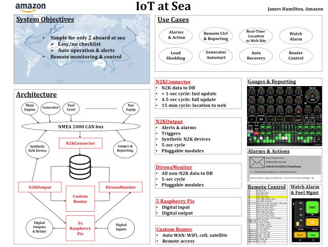
IoT at Sea
In an unusual turn around, rather than have the students attending HTPS do poster sessions, Program Chair Peter Alvaro asked some of the long term attendee to do poster sessions. Peter’s thinking on why the inverted poster sessions would be fun:
As I am sure you already know, poster sessions are a common feature of academic conferences. In a typical poster session, a large group of graduate students assemble in a room, each stationed in front of a 36″ x 48″ printed poster that is organized into rectangular tiles, each of which contains figures, tables, or bulleted text. A larger group of conference attendees, almost always more senior than the presenters, then enter the room and begin to drift among the posters. Armed with wine and cheese, the audience members silently peruse the content, occasionally asking questions. Most questions are of the form: “so tell me about your poster.” The student then attempts to give their elevator pitch. More often than not, the audience member meanders away before the pitch is over. Another audience member drifts in, the student resets their pitch, and the process begins anew. Needless to say, the students are not able to enjoy the poster session as attendees.
For my poster session I chose to cover IoT at sea. This is the software system I wrote for our around-the-world boat tour that supported capturing 100s of data points every 5 seconds from sensors all around the boat weather station, fuel levels, main and auxiliary engine data, generator telemetry, navigation and communications systems data. The system supported generator auto-start, remote reporting and control, managing satellite, cellular, and WiFi communications links, and operator alerting.

- Slides for HPTS Comes Full Circle: https://mvdirona.com/jrh/talksandpapers/JamesHamilton20221010.pdf
- Slides for IoT at Sea: https://mvdirona.com/jrh/talksandpapers/JamesHamiltonHPTS2022Poster.pdf
- More on the Marine IoT System: https://mvdirona.com/2018/04/control-systems-on-dirona/
Thanks James for sharing. I noticed you left out the manufacturing side of semiconductors, something AWS should be preparing for according to your figures.
The ticket for advanced process is priced at 2 billion in R&D budget, and you say AWS is in the hundred millions. 30,000 wafers per month is what competitive fabs require, and your figures suggest that AWS is at 5,000 wafers per month. Summing up, it looks like AWS is just an order of magnitude shy of manufacturing its own chips.
At the speed AWS is growing, this translates into just 2 or 3 years down the roadmap. We haven’t talked about the volume from the consumer side of Amazon, and obviously Apple’s size is already very much compatible with the idea of in-house fabs.
I wonder how open-minded are you towards the last-mile of full-circle innovation, that is semiconductor manufacturing?
That’s an intriguing thought and it’s certainly possible that AWS wafer volumes would someday by large enough to fully utilize an entire fab. For continuity of supply reasons, we would never want to have our entire capacity sourced from a single facility. And, truly large volumes are required to support the R&D investment stream needed to remain a fab leader. Fully utilizing a single fab would be good in the short term but operating sub-scale is a temporarily advantage. Far larger volume — many successful fabs — are needed to stay on top generation after generation. Even some very competent companies with super high fab volumes have fallen more than a generation back. Being a great fab supplier requires the combination of mass volume and excellent leadership. Fortunately, we have a special relationship with TSMC and other leading fab operators and we feel like we are well served but your suggestion is an interesting one.
Thanks James for sharing your thoughts. As a happy T4 and T3 Graviton customer, it’s great to learn that AWS is taking a comprehensive approach towards the semiconductor space.